Because wire bonding creates strong and reliable connections between an IC die and the package that houses it, it is critical to semiconductor functionality. This application focuses on inspecting semiconductors for wire bond defects.
What manufacturing defects occur?
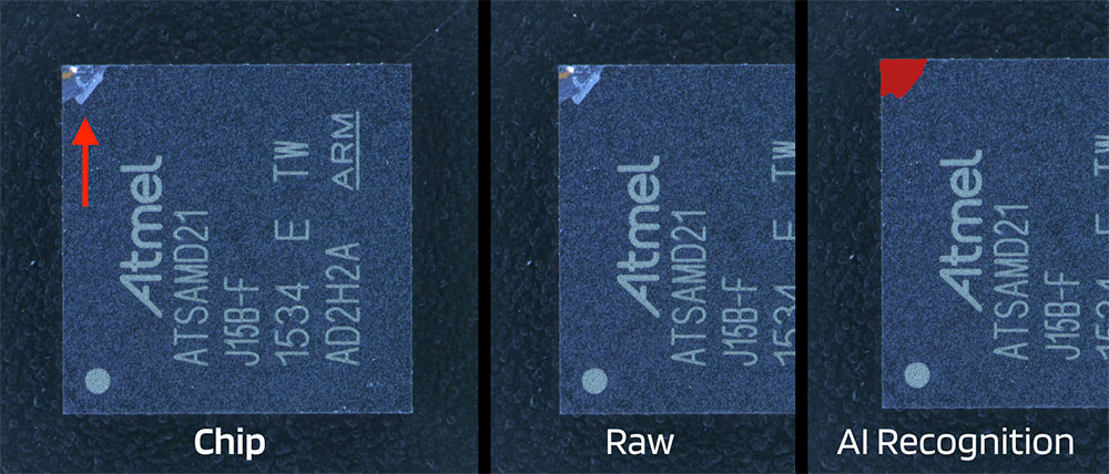
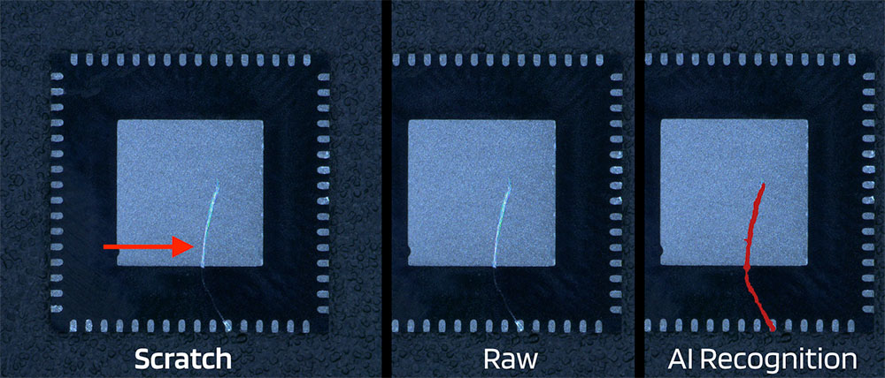
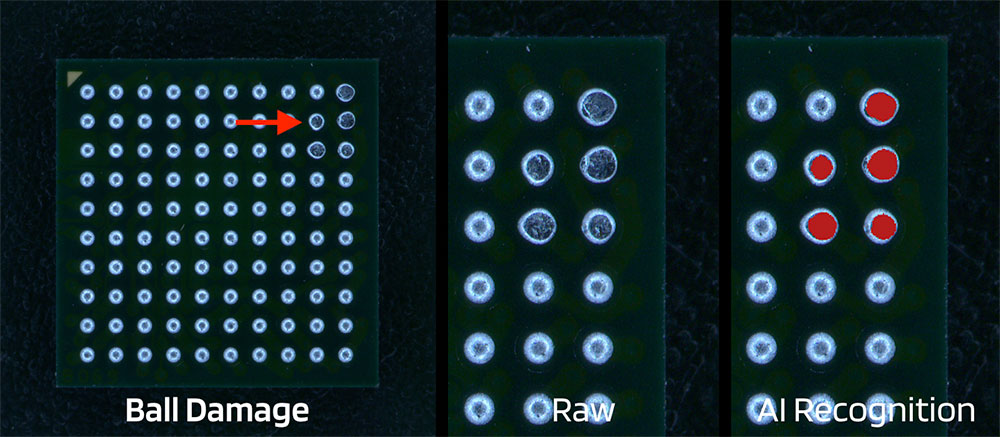
However, wire bonding is a delicate manufacturing process that can result defects such as:
Because such defects can affect the functionality and reliability of the final device and even cause complete failure, wire bonding must be meticulously controlled and inspected.
Implementing robust inspection practices and quality control measures are crucial for mitigating these risks and ensuring the production of reliable and safe semiconductors.
But wire bond defects are challenging to detect– they can be subtle, complex, and variable in type and location. Traditional machine vision requires programming hundreds of hand-crafted rules and fail to detect new or variable defects that don’t match their programmed parameters. Wire bond materials are reflective, making defects hard to see. Both manual inspectors and traditional machine vision systems can fail to distinguish between reflective surfaces and actual defects, causing both false positives and escapes.
The Solution
UnitX’s AI-powered inspection effectively detects wire bond defects where other solutions fail.
First, the OptiX imaging system illuminates and images wire bonds. Then, the CorteX AI platform is trained on wire bonding defects. Lastly, those AI models are deployed to the CorteX inference system to detect and classify defects in-line.
Why UnitX for wire bond inspection?
OptiX provides superior images that minimize reflectivity while maximizing defect visibility. It has 32 independently controllable lighting sources that can be optimized for wire bond surfaces and various defects via software. Its computational imaging capability can be used to take multiple shots and eliminate hotspots caused by highly reflective wire bond surfaces. And its lighting dome design supports a very acute incidence angle of projected light, causing even very tiny defects to cast shadows which increase their visibility.
CorteX accurately detects random, complex defects. It automatically normalizes for variability in positions and orientations and recognizes defects down to the pixel-level.
UnitX supports fast experimentation and adapts to changes in production environments. OptiX lighting is easily configured via software and CorteX AI models are sample efficient– they only require a few images to train on new defect types.
UnitX provides rapid, 100% inline inspection. OptiX has bright LEDs and fast fly capture speeds of 1m/s for high speed imaging. And CorteX supports high inference speeds (up to 100 MP) to quickly output an OK/NG decision, seamlessly communicating that decision via integration to all major PLC, MES, and FTP systems.
With UnitX, manufacturers prevent wire bond defects and avoid chip failures, reliability reduction, and reputational impacts as a result. They automate inspection at the speed of their production to increase semiconductor chip throughput and yield.